Turnkey
-
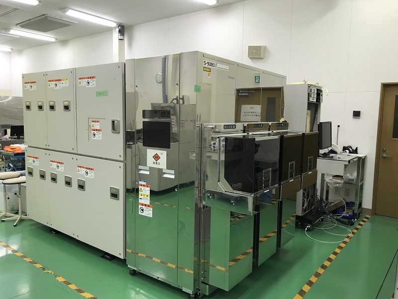
Hitachi S9380 CDSEM
Wafer size: 300mm or 200mm SEMI or JEIDA standard orientation flat or V notch wafers
Resolution: 2nm (Accelerating voltage: 800V)
Magnification: x1100 (Optical Microscope), x1,000 ~ 300,000 (SEM)
Measurement system: Cursor and line profile
Measurement range: 0.05 ~ 2.0 μm
Repeatability: +/- 1% or 0.6nm (3 sigma) (with Microscale sample)
Objective lens: High Excitation low aberration lens
Accelerating voltage: 300 ~ 1,600 V (10V Step)
Auto-loader: 2 or 3 FOUPs random access
Throughput: 24 wafer/hours (20-measurement points on wafer)
-
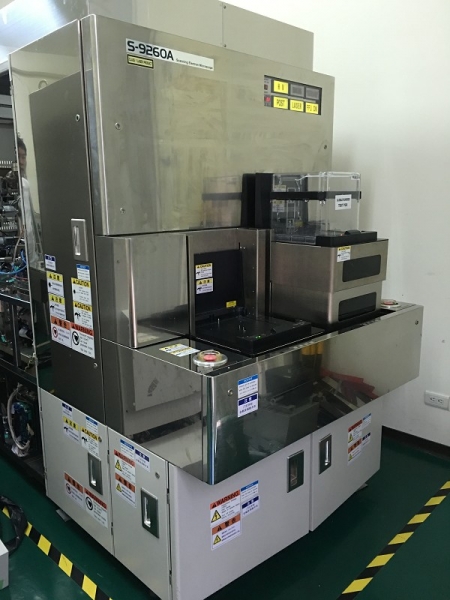
Hitachi S9260 CDSEM
Wafer size: 300mm or 200mm SEMI or JEIDA standard orientation flat or V notch wafers
Resolution: 3nm (Accelerating voltage: 800V)
Magnification: SEM Image; 500x to 300,000x
Measurement range: 0.1 ~ 2.0 μm
Reproducibility:: +/- 1% or 2nm (3 sigma), whichever larger
Auto-loader: 2 or 3 FOUPs random access
Throughput: 65 wafer/hours (in continuous measurement via recipe, under Hitachi standard test conditions), 1 point/chip, 5 chips/wafer

-
Hitachi S9220 CDSEM
Wafer size: 200mm or 150mm SEMI or JEIDA standard orientation flat or V notch wafers
Measurement method: Curser or line profile method
Measurement range: 0.1μm ~ 2.0μm
Measurement repeatability: ±1% or 2 nm(3 Sigma), whichever larger
Throughput:
S-9220; 56 wafers/hr (in continuous measurement via recipe, under Hitachi standard test conditions)
S-9200; 45 wafers/hr (in continuous measurement via recipe,
under Hitachi standard test conditions)
Measured points; 1 point/chip, 5 chips/wafer
Secondary electron image resolution: 3nm (at accelerating voltage of 0.8 kV; with OEM reference specimen for resolution measurement)
Image magnification: 500 ~ 300kx
-
Hitachi S8820 CDSEM
Wafer size: 200mm or 150mm
Principle of CD measurement: Cursor and line profile measurement
CD measurement range : 0.1 to 10μm
Measurement Repeatability: ±1% or 0.005μm (3 sigma)(threshold method), whichever larger
throughput: 26 wafers/hour (in continuous measurement), 1 point/chip, 5 chips/wafer
Secondary electron image Resolution: 5 nm (50 A) (at accelerating voltage of 0.8kV) (with reference specimen dedicated for resolution Measurement)
Magnification: ×1000 to ×150,000(SEM image), About×110(optical microscope image)
Option: modification to 6” or 4” GaAs wafer.